-
Description
Semiconductor Optical Amplifiers (SOAs) are of great interest for switching and gate applications
in WDM-based optical networks since they allow very high on-off switching ratios and can provide, in addition, broadband
signal amplification. However, the gain saturation in conventional SOAs generates interchannel crosstalk which severely
limits their usage in WDM-based systems. Moreover, fast gain dynamics in SOAs in conjunction with gain saturation may
generate intersymbol interferences, leading to signal distortions even in single-channel systems. To overcome these
limitations gain-clamped SOAs (GC SOAs) have been proposed and fabricated in the last decade. In GC SOAs, the optical
gain is clamped by a lasing mode generated outside the signal band. The gain-clamping lasing mode can be introduced, for
example, by attaching either passive distributed Bragg reflectors (DBRs) or active
distributed feedback (DFB) structures to the ends of the active section [1]. As a result, the gain in GC SOAs remains constant with respect to input power
variations as long as the amplified signal power is less than a certain critical power, leading to a flat gain versus
output power response.
-
Typical Results
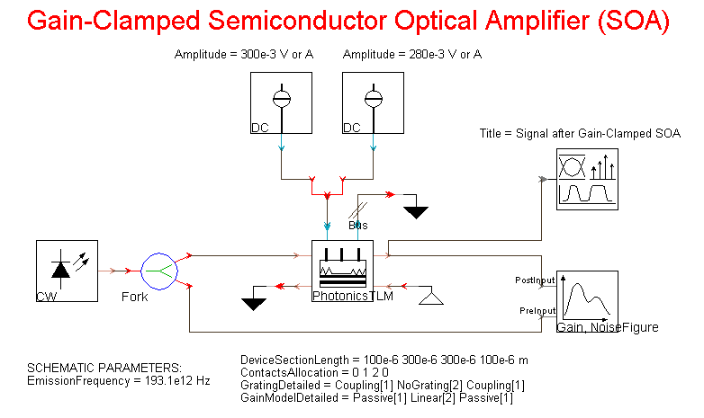
The simulation setup illustrating the design of a GC SOA is shown in
. The GC SOA in
this example consists of a two-contact active section surrounded by two DBR sections. The first 300 µm of the
active layer are injected with 300-mA current while the subsequent 300 µm layers are injected with 280 mA. The
length of each DBR region is 100 µm. The idea of such a two-contact GC SOA has been suggested in [2]; using two
contacts in the active layer allows improving the gain flatness of the SOA significantly. Parameters of the active layer
correspond to the SOA parameters employed in [3].
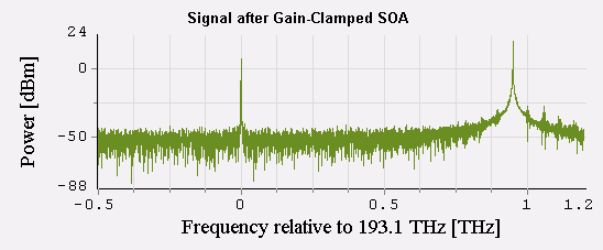
shows the signal
spectrum after passing the GC SOA. It can be noticed that in addition to the amplified signal at 193.1 THz, the GC SOA
generates a lasing mode at 194.1 THz which is responsible for the desired gain clamping.
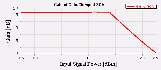
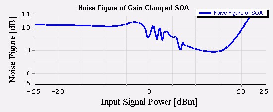
and
represent the
dependences of the gain and noise figure of the modeled GC SOA on the input signal power. Remarkably, the observed
variations of the gain do not exceed 0.05 dB for the input signal powers up to 0 dBm. The noise figure of the modeled
GC SOA does not exceed 10.5 dB. It can potentially be reduced to around 7 dB by employing unbalanced Bragg reflectors [4].
The module PhotonicsTLM employed in this setup permits to model various advanced SOA designs with multiple sections of
different types, including, for instance, bulk and MQW active layers, DFB and DBR sections, and multiple contacts for injection currents.
-
Further Information
Keywords: Semiconductor Optical Amplifier (SOA), Gain-clamped SOA (GC SOA), Gain Flatness, SOA in WDM systems
Similar demonstrations are available in VPIComponentMaker Photonic Circuits and on the VPIphotonics Forum.
[1] D. Wolfson et al., IEEE Photon. Technol. Lett. 10 (9), 1241-1243 (1998)
[2] J. Park et al., IEEE J. Quantum Electron. 39 (11), 1415-1423 (2003)
[3] T. Durhuus et al., J. Lightwave Technol. 10 (8), 1056-1065 (1992)
[4] G. Guiliani and D. D'Alessandro, J. Lightwave Technol. 18 (9), 1256-1263 (2000)