
VPIphotonics offers consulting services for creating customized library extensions to VPIcomponentMaker Photonic Circuits providing circuit-level support of a Process Design Kit (PDK) for various integrated photonics technologies (Indium Phosphide, Silicon, Silicon Nitride, Polymer).
These pluggable toolkits support a cost-effective generic foundry approach for
application-specific photonic integrated circuits (ASPICs) design. Within this approach,
the user or the system designer can choose photonic devices from a fixed list of so-called
building blocks (BBs) supported by the individual foundry. Each BB is characterized by only
a few user-defined parameters and is represented with an adequate simulation model.
Each VPItoolkit PDK <fab> allows the user to rapidly prototype ASPICs with prerequisite
functionality utilizing foundry-specific information without going deep into the details of device
layout and fabrication process of that specific foundry.
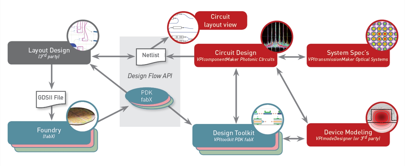
Integrated design flow for photonic circuits
Importantly, VPItoolkit PDK <fab> implements the novel layout-aware schematic-driven PIC design methodology [1]. In terms of this methodology, the circuit-level simulator supports the capability to specify exact physical locations and orientations of PDK BBs on the final layout (when this is required by DRC and packaging specifications) and to connect sub-circuits having fixed locations by smart elastic optical connectors.
This allows to combine graphical schematic capture and automated waveguide routing,
which are currently considered separately and represent a major problem for PIC designers.
Key enabler for this functionality is the seamless integration of circuit and layout tools:
VPIcomponentMaker Photonic Circuits extended by a VPItoolkit PDK <fab> automatically
and invisibly for users invokes a layout design tool
(PhoeniX OptoDesigner by Synopsys,
IPKISS by Luceda Photonics or
Nazca Design)
to determine the actual physical lengths and shapes of all elastic connectors, constructs
compact simulation models for them, and after that initiates the circuit simulations.
[1] PIC Magazine Issue 4 – "PIC Design: schematic or layout first? Both!"
[2] VPIphotonics-Luceda Whitepaper
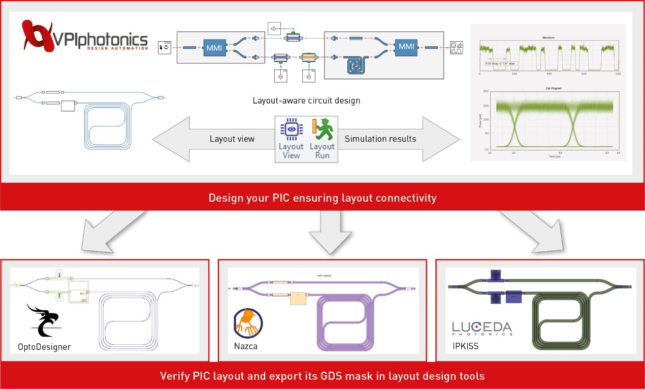
Intermediate and final circuit design solutions can be exported automatically to PhoeniX OptoDesigner,
IPKISS [2] or Nazca to fit the layout to the die package, add proper electrical wire routing, perform
design-rule-check (DRC) verification, and generate a GDS mask for circuit fabrication.
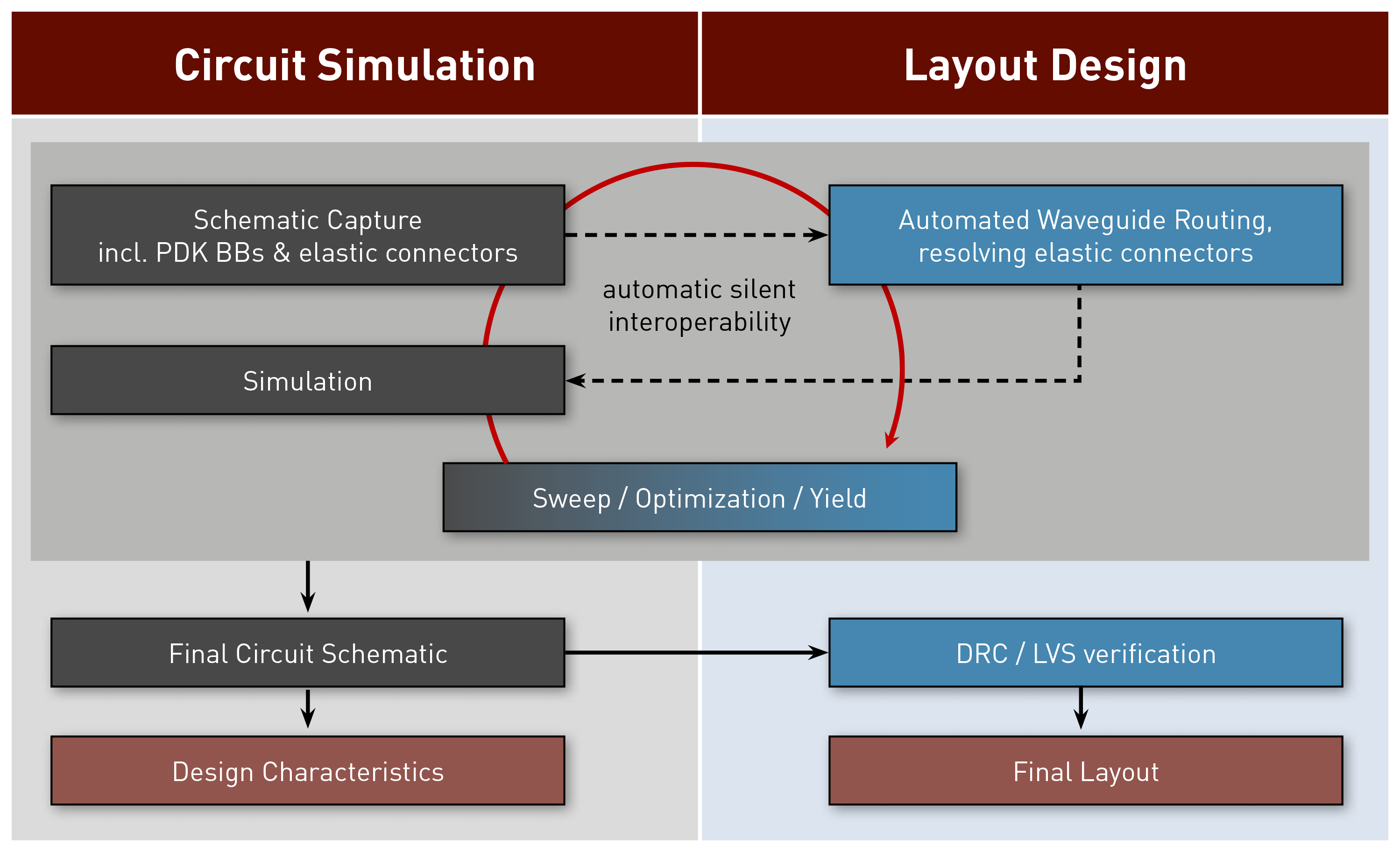 Sketch of layout-aware schematic-driven design methodology
Prototype integrated photonics and optoelectronics circuits with prerequisite functionality
Account for layout information (physical locations, orientations) of BBs in the circuit design
Utilize rich libraries of passive and active BBs which can be fabricated at the foundry
Extended library of advanced elastic optical connectors, which provide automated waveguide routing capabilities to the circuit level simulator
Optimization of the designed circuit using standard VPIcomponentMaker Photonic Circuits instrumentation
Analyze fabrication tolerances and yield performance, and compare technology alternatives
Build on adequate simulation models of BBs that are based on characterization data
Seamless integration into VPIcomponentMaker Photonic Circuits
Support of PDAflow API
Support of fast layout top view for designed optical chips in absence of external layout design tools
Export the circuit to PhoeniX OptoDesigner, IPKISS or Nazca for layout, packaging and GDSII mask generation
All the building blocks supported by VPItoolkit PDK <fab> can be used alongside with a
broad set of standard modules and instrumentation in
VPIcomponentMaker Photonic Circuits.
 Simulation workflow for running schematics with elastic connectors
Advanced libraries of standard modules, including:
Passive and active components with thoroughly tested and extensively documented physical models
Optical and electrical signal sources
Open interface for experimentally measured or numerically calculated device models
Flexible design and modeling capabilities, including:
Unique hybrid time-and-frequency-domain modeling (TFDM) approach for large-scale active photonic integrated circuits
Hierarchical design approach
Python, Matlab and C++ cosimulation
Embedded layout view
Setup & Layout Export in PhoeniX OptoDesigner

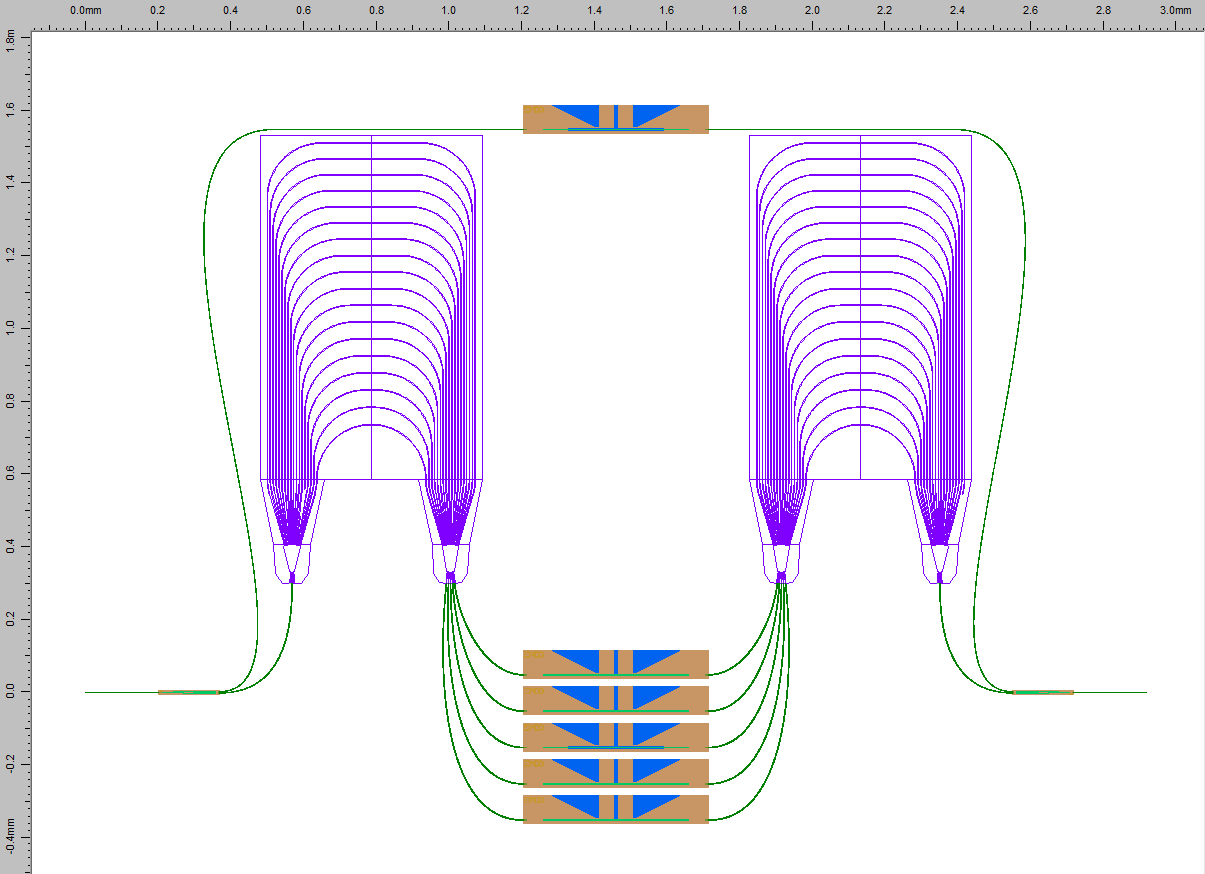
Circuit design using VPItoolkit PDK DemoFab (PhoeniX OptoDesigner)
Export of photonic circuit designs into PhoeniX OptoDesigner
Setup & Layout Export in IPKISS
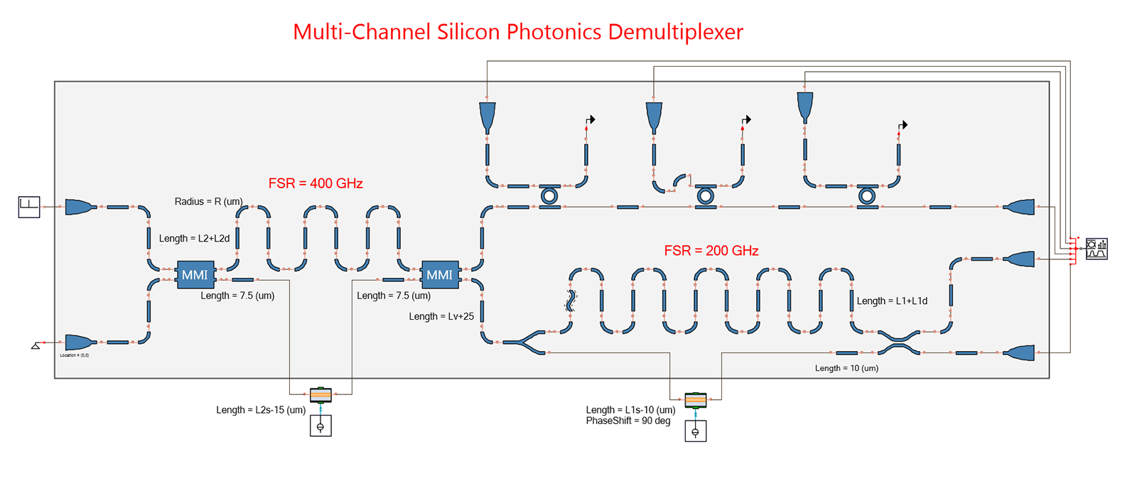
Circuit design using VPItoolkit PDK DemoFab (IPKISS)

Export of photonic circuit designs into IPKISS
Setup & Layout Export in Nazca
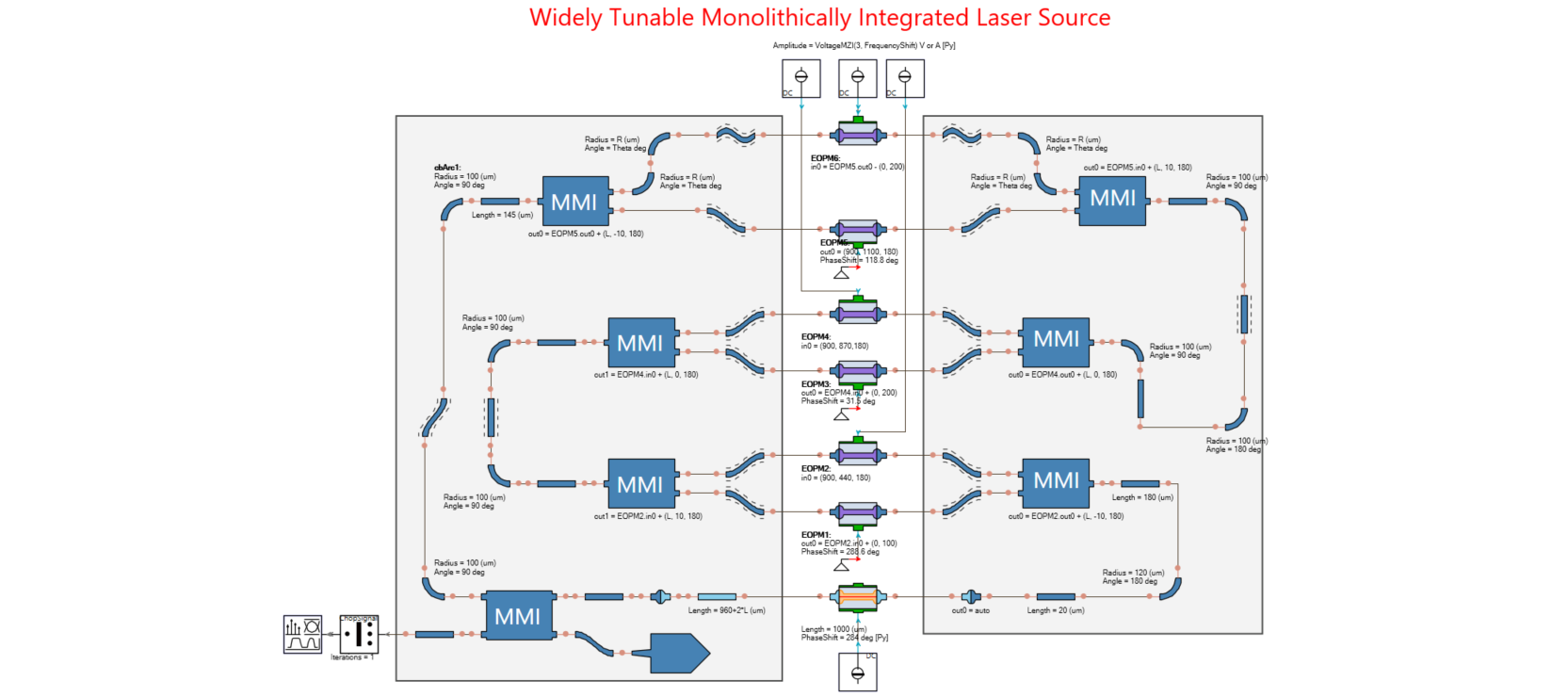
Circuit design using VPItoolkit PDK SMART (Nazca)
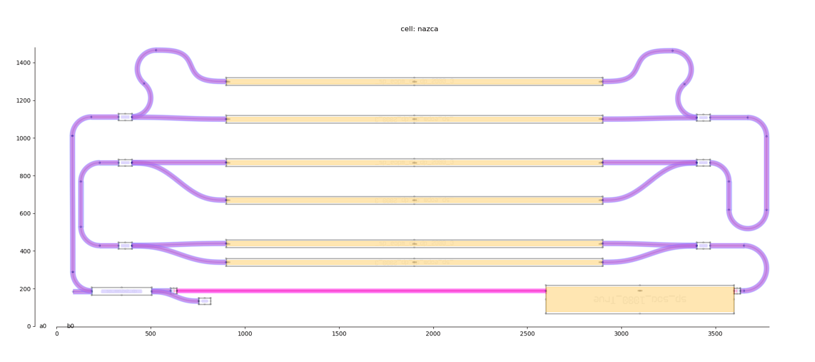
Export of photonic circuit designs into Nazca