


The European Conference on Integrated Optics (ECIO) has now
reached its 19th edition. Innovation and industry uptake is accelerating, and to capture this increasing pace, we are now transitioning to
an annual event.
In 2017 we return to Eindhoven at the Science Park of the TU Eindhoven. We will retain the same clear focus on
leading edge research, providing a forum for experts from industry and academia to share the latest new thinking and exchange new insights
and findings in the fields of integrated optics, optoelectronics and nanophotonics.
The conference scope extends from new enabling materials to the design & modelling of photonic structures, functions, devices and
circuits. We also capture innovations in hybrid integration, SoC & system-in-package integration. Application areas range
from optical communications; interconnects, switching & storage; data & information processing, including
integrated quantum circuits; and optical monitoring & sensing, including mid-IR photonics.
The Optical Wave and Waveguide Theory and Numerical
Modelling (OWTNM) workshop has, yearly since 1992, provided a forum for lively debates, intended to bring forward new ideas in the field of
theoretical and computational photonics.
Basic physics and novel applications, artificially structured materials and new devices, elegant mathematical techniques and efficient
numerical methods to tackle the Maxwell equations form the constantly evolving subjects. These are discussed in a traditionally open and
relaxed atmosphere.
Topics of interest for the workshop on Optical Wave and Waveguide Theory and Numerical Modelling address the physical understanding, the
mathematical description, and the computational treatment of guided as well as non-guided optical waves and related effects in micro- and
nanostructures.
Thu 6th 11:40-12:00 AM, OT2.3
Abstract: In this paper, a novel modelling method for 3D multimode interference (MMI) structures is presented. We have demonstrated the physical model and performance of a 16x16 3D MMI. The simulation results are based on self-imaging phenomena in multimode waveguides.
A. Polatynski ¹, S. Mingaleev ¹, A. Marinins ², D. de Felipe ³, M. Kleinert ³, M. Kresse ³, C. Zawadzki ³, N.Keil ³, A. Richter ¹New Version: VPIphotonics Design Suite™ v9.8
Design Photonic Components and Compare Transmission Technologies
VPIphotonics Design Suite accelerates the design of new photonic systems and subsystems for short-range, access, metro and long-haul optical transmission systems. Further, it supports assessment of technology upgrade and component substitution strategies that are to be developed for existing fiber plants. Highlights supported by the new version 9.8:
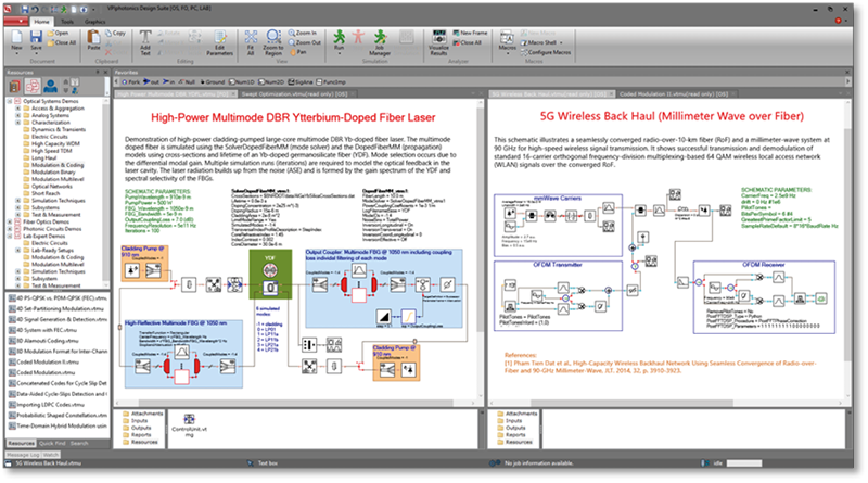
Live Demos: Rapid prototyping with Photonic PDKs
Pluggable toolkit extensions to versatile circuit simulation environment support MPW runs at Fraunhofer HHI, LioniX and SmartPhotonics
Live Demos: Automated design methods for photonic ICs
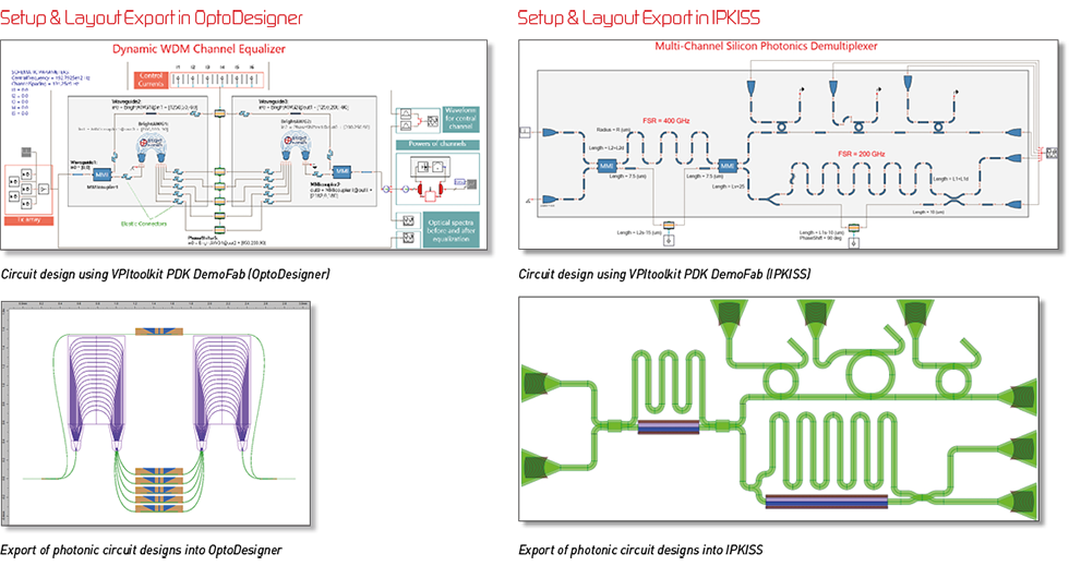
Layout-aware schematic-driven design with VPIcomponentMaker Photonic Circuits and its seamless interfaces to OptoDesigner by PhoeniX Software and IPKISS by Luceda
VPIcomponentMaker Photonic Circuits integrates with OptoDesigner by PhoeniX Software and IPKISS by Luceda via pluggable toolkit extensions. These interfaces enable the novel layout-aware schematic-driven design of photonic and optoelectronic integrated circuits. This approach greatly simplifies and accelerates the design workflow, providing an automated export of photonic circuit designs into OptoDesigner or IPKISS for layout design finalization and mask generation.
Set up an appointment with one of our experts for a customized presentation.